
Maurice Tutor
$15/per page/Negotiable
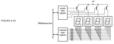
A Gumnut system includes a 4-digit 7-segment display, connected as shown in Figure 8.45. The anode data register is at port address 128, and the cathode data register is at port address 129. Write Gumnut assembly code for the task_2ms subroutine described in Example 8.17 on page 369 to scan the display. The BCD digits to display are stored in four bytes of memory labeled display_data. The subroutine should select one digit to drive each time it is called. Thus, four successive calls are required for a complete scan.
Example 8.17
Suppose a Gumnut system includes the real-time clock controller of Example 8.16 with the registers located at base port address 16. Develop Gumnut code that calls the subroutine task_2ms every 2ms. In between activations, the program stands by in low-power mode. The subroutine should not be called as part of the interrupt handler, since other interrupts should be permitted during execution of the subroutine.
Example 8.16
Develop a Verilog model for a real-time clock controller for the Gumnut processor. The controller has a 10µs time base derived from a 50MHz system clock, and an 8-bit output register for the value to load into the counter. A write operation to the output register causes the counter to be loaded. After the counter reaches 0, it reloads the value from the output register and requests an interrupt. The controller has an input register for reading the current count value. The counter also has a 1-bit control output register. When bit 0 of the register is 0, interrupts from the controller are masked, and when it is 1, they are enabled. The counter has a status register, in which bit 0 is 1 when the counter has reached 0 and been reloaded, or 0 otherwise. Other bits of the register are read as 0. Reading the register has the side effect of acknowledging a requested interrupt and clearing bit 0. The counter output and input registers are located at the base port address, and the control and status registers are at offset 1 from the base port address.
Â
Â
Â
Â
Â
Â
Â
Â